AB INITIO
Back
Last month we looked at how a semi-conductor “p-n junction” in a simple rectifier diode worked, and how it relied on two different kinds of charge carrier, electrons and holes in the ‘n’ and ‘p’ types respectively of a semi-conductor. As both types of charge carrier thermally diffuse a short distance into the opposite sort of semiconductor, mutual annihilation of both types occurs at the interface. The net result is that an insulating or “depletion region” between the two types is set up, across which a small potential difference exists, (because of the diffused charges). The diode article contained a diagram which is reproduced in figure 1. This shows the charge carriers as +s and –s, (but not the positive nuclei of the host atoms), and the direction of the electric field between the ‘n’ and ‘p’ regions in the absence of any applied voltage.

The potential difference resulting from this internal electric field is of the order of a half to one volt. However, when an external voltage is applied, this potential barrier either rises, to make it impossible for current to flow, or falls enabling it to be easily overcome depending on which way the external voltage was applied. Hence the p-n junction acted as a valve, only allowing current to flow in one direction, from the ‘p’ to the ‘n’ regions. A rather crude analogy might be keeping out the sea by a sea wall, where the small potential difference across the depletion region represents a small difference in height between the sea level and the top of the sea wall. In this analogy, the wind represents the externally applied electric field. When the wind is blowing from the land to the sea, the sea is kept below the top of the sea wall, corresponding to no flooding and no current. When the opposite occurs, and the wind blows from the sea to the land the sea level rises and it has only to be a few inches higher than the top of the sea wall for “the flood gates to open” and a torrent of water floods over it onto the land, corresponding to a large current flowing. These principles need to be firmly understood, (by analogy or otherwise), to understand the next step: the transistor.
There are many different kinds of transistor and transistor-like devices which go under a variety of names such as: Bipolar Transistors, (which were the earliest to come into common use), Field Effect Transistors, (junction and insulated gate types), Thyristors, Diacs and Triacs, and others. The action of all of them is that a small amount of energy controls the flow of a large amount of energy. The action of some can be likened by analogy to controlling the powerful flow of water from a hosepipe by standing on it and therefore reducing its cross sectional area. Analogies are useful but must not be taken too far, and they often leave more questions unanswered than they answer.
The first commercial transistors were “bipolar”, and the action or mechanism of operation of these is probably the most difficult to explain, whether by analogy or otherwise. This is the type whose action I shall attempt to explain as the action of many of the others follows on from this.
The Transistor
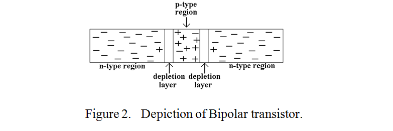
The bipolar transistor consists of two p-n junctions back to back as depicted in figure 2. (It is called bipolar because it makes use of two types of charge carrier; electrons and holes).

Whichever way an external supply voltage is connected between its ends, no current can flow because one of the p-n junctions will always be reverse biased. Now consider what happens when one of the p-n junctions is forward biased by a small voltage, shown as a single cell in figure 3.

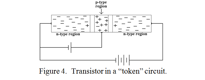
The left hand p-n junction is forward biased and electrons flood over its depletion region into the p-type region. Because they are being driven by an applied voltage, they will move much faster than the original thermal diffusion electrons and many of them will overshoot the p-type region and the next depletion region before being dragged back by the small applied voltage into the positive terminal of the single cell. Now consider that a positive voltage is applied to the right hand end of the right hand n-type region as depicted in figure 4.

The flood of electrons which overshot the p-type region and the right hand depletion layer now find themselves in a conducting region and are attracted to an even higher positive voltage from the second external battery. If the p-type region is made fairly thin, (compared with the average natural diffusion distance of thermal electrons), the number of electrons which overshoot the p-type region can be a couple of orders of magnitude greater than those attracted by the positive terminal of the single cell shown in figures 3 and 4. Even though the right hand depletion region is comparatively wide due to the reverse bias of its p-n junction by the second battery, the electrons which enter it keep going under the influence of the right hand battery. The transistor therefore has “current gain”. I.e. a small change in current through one p-n junction causes a large change in the end to end current through the transistor.
It should be noted that figures 3 and 4 are “token” circuits. A suitable resister should always be incorporated in series with the emitter-base p-n junction as the voltage from any normal cell greatly exceeds the natural p-n junction field voltage. Without such a resistor a very large current would flow through the junction thus destroying it.
Terminology
The circuit symbol for an n-p-n transistor, (the commonest type), is shown in figure 5 below.

The transistor connection which emits the main charge carriers, (in this case electrons), is called the “emitter”, the central, (p-type), region is called the “base”, and the connection which collects the main charge carriers, (electrons again), is called the “collector”.
PRAECEPTOR
| Back |
|---|
